This research has developed DSP-based digital control techniques for high-performance single-phase on-line UPS systems. A transformerless common-neutral half-bridge AC-DC-AC converter has been adopted for the main power circuit. All the control functions for an on-line UPS, which includes power-on start-up control, input stage power factor control, battery charging and boosting control, output stage ac voltage regulation, and shut-down control, were realized by using a single-chip DSP controller, the TMS320F2407A. A multiple rate digital controller generates all the PWM control signals for the power stage by using a set of synchronously detected feedback signals. Software current control scheme with nonlinear pulsewidth compensation has been developed to eliminate the nonlinearity caused by the dead-lock protected PWM converters. A nonlinear digital control scheme with lower switching frequency has been developed for the power factor control of the ac-dc converter. Computer simulation and experimental results have been given to verify the proposed digital control scheme. The constructed DSP-controlled UPS system can achieve fast dynamic response for nonlinear loads and high power factor under various loading conditions. The developed UPS digital control techniques have been applied to a commercialized single-phase 2 kVA double conversion UPS. Excellent performance measurements have been achieved in the designed DSP-controlled UPS.
Implementation of a fully digital-controlled UPS provides many advantages, such as more sophisticated control functions can be employed in a UPS system, a software-controlled UPS can be more flexible, advanced robust control schemes can be implemented to accommodate stringent and versatile application requirements. Many research works have been carried out on the closed-loop regulation of PWM inverters using various feedback control schemes to achieve both good dynamic response and low harmonic distortion. Microprocessor-based deadbeat control technique has been applied to the closed-loop regulation of PWM inverters. Deadbeat control has been developed for the voltage regulation of the PWM inverter by employing a minor current loop and a major voltage loop. However, deadbeat control scheme has the disadvantages of highly sensitive to parameter and load variations and requiring large peak-to-average ratio of control signals to achieve deadbeat effect.

With the great advances in microelectronics and VLSI technology, high-performance microprocessor and digital signal processors (DSPs) can be effectively used to realize advanced control schemes [7]. Most instructions of a DSP can be accomplished within one instruction cycle and complicated control algorithms can be executed with fast speed, therefore, more control functions can be realized by using software. Attempts have been made to realize a fully DSP-controlled UPS [8]-[9]. However, only limited functions have been realized using software. In this paper, a single-chip DSP controller, the TMS320F240 from Texas Instruments, has been used to realize all the control functions required in an on-line UPS system.
With the availability of 16/32-bit high-performance single-chip DSP, as shown in Fig. 1.3, most of its instructions can be accomplished within one instruction cycle, complicated control algorithms can be realized efficiently. This paper describes the design and implementation of a DSP-embedded fully digital-controlled single-phase on-line uninterruptible power supply (UPS) system. All the control functions for an on-line UPS, which includes power-on start-up control, input stage power factor control, dc-link voltage regulation, battery charging and voltage boosting control, output stage ac voltage regulation, and shut-down control, were realized by using a single-chip DSP controller.
2. Power Circuit Design
The selection or development of a circuit topology for a single-phase double-conversion UPS plays a most important role in the design of a high-performance UPS. This is due to that the circuit topology is highly dependent on the overall efficiency, cost, safety regulations, and possible patent conflicts

Single-ended, half-bridge, or full-bridge PFC converters are all boost converters, from the point-of-view of control loop design they have the same dynamics. The only difference is the effective voltage applied to the inductor due to a specified PWM duty. From the point-of-view of power circuit design, these three PFC converters have the same utilization factor, which result the processing power ratings are proportional to their number of switches. The half-bridge PFC converter has advantages of common-neutral in UPS applications and a minimal number of power switches is required. However, it also has disadvantages of higher voltage stress and need fast response balance control of the totem-pole capacitor bank. Fig. 2.2 shows the detailed schematics of the power circuit of the common-neutral ac-dc-ac converter and Fig. 2.3 is an illustrated circuit topology for functional description and component rating calculations.

Figure 2.3 Common-neutral half-bridge ac-dc-ac converter.

Figure 2.2 Schematics of the Common-neutral half-bridge ac-dc-ac converter.
The inherent bi-directional characteristics of a common-neutral ac-dc-ac converter can be illustrated as shown in Fig. 2.4. The UPS output connected load may be inductive, capacitive, or even nonlinear with reactive characteristics, therefore, in order to a unit power factor input as well as keep a good dynamic response under step load change condition, the dc-link capacitor should provide a sufficient energy storage to maintain a half-cycle voltage fluctuation.

Single-ended, half-bridge, or full-bridge PFC converters are all boost converters, from the point-of-view of control loop design they have the same dynamics. The only difference is the effective voltage applied to the inductor due to a specified PWM duty. From the point-of-view of power circuit design, these three PFC converters have the same utilization factor, which result the processing power ratings are proportional to their number of switches. The half-bridge PFC converter has advantages of common-neutral in UPS applications and a minimal number of power switches is required. However, it also has disadvantages of higher voltage stress and need fast response balance control of the totem-pole capacitor bank.
3. Control Loop Design
There are many control functions required in a smart UPS system, These may include system monitoring, diagnosis, protection, interface control, and real-time control. The real-time control function plays an important role for the improvement of the UPS control performance. The control functions of a UPS system can be classified four major parts according to their control purposes. These include: front-end power factor correction control, PWM inverter control for sinusoidal output voltage regulation, the dc-dc boost control for dc-link voltage regulation, and the battery charging control. These control functions are described as follows.3.1 Power Factor ControlRegulations on line current harmonics have made power factor control a basic requirement for power electronic equipment [14]. The main purpose of the PFC converter is to shape the input current to be linear proportional to its input voltage so that it behaves as a resistor. Another purpose of the PFC converter is to regulate its output dc voltage under line and load variations.Conventional PFC control schemes focus on the shaping of the line current in proportional to the voltage and therefore, a current loop controller with wide bandwidth is required. However, in order to minimize the current distortion resulted from the dc-link voltage regulation, a low-pass filter is required to smooth the double line frequency ripples in the dc-link voltage. This results a slow response of the UPS front-stage power converter. The slow response of the PFC converter will result a large voltage drop under a step load change and further deteriorate the UPS output waveform.In order to improve the dynamic response of the PFC boost converter, various feedback control schemes have been analyzed in [15]. Analog notch filter to eliminate measured output voltage ripples can achieve a better dynamic response compared with other approaches. Development of fast response control schemes for the PFC boost converter has become a technical pursuing goal in recent years [16]-[19]. These control techniques break the bandwidth barrier of double line frequency by using sophisticated control techniques in elimination the influences of output voltage ripples. All these control schemes are applied to the PFC boost converter and using analog controller or analog current-loop controller with microprocessor-based voltage-loop controller.One major design challenge in synthesizing a digital PFC controller is that we must make a compromise between the line current distortion and a fast response of the dc-link voltage regulation. Fig. 3.1 shows the control structure of a single-phase PFC converter and Fig. 3.2 is the detailed control block diagram. The PFC controller consists of three sub-controllers: an inner current loop controller, an outer voltage loop controller, and an adaptive ripple estimator.The inner current loop controller is required to regulate the line current with a high sampling rate, usually from 10 to 20 kHz. The outer voltage loop controller is used to regulate the dc-link voltage and at the same time to generate a current reference for the current loop. A lower sampling rate from 1 to 2 kHz is an appropriate choice for the voltage loop. The adaptive voltage ripple estimator is used to generate a compensated signal to cancel the line ripple voltage occurred in the dc-link.


3.2 PWM Inverter Control
The control loop design for the PWM inverter for ac voltage regulation is most difficult in the synthesis of the digital controller for the UPS. This is due to that the inverter should provide good quality ac voltage, this means low voltage THD, for various kinds of loads. The control architecture of the PWM inverter for ac voltage regulation is shown in Fig. 3.3. It includs four control loops.
- Balancing Control Loop (fs=60 Hz): This loop is used to compensate dc-offset due to nonlinear distortion such as unbalanced turn-on and turn-off time, unbalance of the upper and lower common-neutral dc-link voltages, and possible dc-offsets of the feedback sensing circuits.
- RMS Control Loop (fs=60 Hz): This loop is used to compensate RMS voltage errors due to limited voltage loop bandwidth and output voltage THD distortion when connected with nonlinear loads.
- Voltage Control Loop (fs=6 kHz): This loop is used to compensate the instantaneous output voltage to track a sinusoidal 60 Hz reference. The desired closed-loop bandwidth (600 Hz) should be at least ten times of the reference frequency (60 Hz). A 10 times of sampling frequency to BW ratio means the voltage loop sampling frequency should be 6 kHz.
- Current Control Loop (fs=24 kHz): The current loop plays a most important role in the control of a PWM inverter for ac voltage regulation. This loop can decouple the inductor from the LC filter dynamics and eliminate nonlinear distortion due to dead-time of the PWM inverter.
 Figure 3.3 Control architecture of the PWM inverter for ac voltage regulation.
- The current loop controller can decouple the nonlinear dynamics resulted by the load. The dynamics of the UPS inverter output filter with its connected load exhibits large load variations. Fig. 3.4 shows the frequency responses of the inverter with resistor load (10% ~100% load). It can be observed that the frequency response exhibits highly resonant characteristics at resonant frequency of the output filter when in light load. In order to achieve good dynamics responses and maintain good stability under large nonlinear load variation conditions, an adaptive variable structure control scheme, as shown in Fig. 3.5, has been developed for the PWM inverter for robust ac voltage regulation.
 Figure 3.5 Block diagram of the digital adaptive variable structure control scheme for AC voltage regulation.
- 3.3 DC-DC Booster ControlThe booster in a UPS system is used to convert the battery output voltage to a much more high dc-link voltage. The battery booster in the designed UPS system is a common-neutral current-fed flyback converter with a coupled transformer. The PI control scheme has been applied for the inner current loop control of the boost converter. Because the booster output is connected to the dc-link and is activated when the utility is failed, its dynamic response behaves as an important performance index. The current-fed flyback converter is current regulated an inner-loop analog PWM controller and voltage regulated by an outer voltage loop controller using PI control with dc-link voltage feedforward compensation.3.4 Battery Charger ControlThe battery charger in the designed UPS system is symmetric common-neutral flyback converter. A proportional controller is used for the current regulation and a simple PI controller is used for the voltage regulation. Constant current with battery voltage profile control is adopted as the battery charging scheme. The charging profile is stored in the EEPROM of the UPS controller and can be reloaded when a new set of battery are installed. The software control approach provides great flexibility in implementing various intelligent battery charging and discharging control schemes.3.5 Line Frequency Synchronization ControlFor a double-conversion UPS, its output voltage must always be synchronized with the line voltage. This design requirement is required because in case of UPS failure or manually switched to maintenance mode the UPS output must be transferred to the line input and the synchronization ensures a smooth voltage transfer. If the line frequency is within the specified output frequency range (±3%), the output voltage should synchronize with the input voltage with zero phase error. However, if the line frequency deviation is larger than ±3% for a specified time interval (such as 10 cycles), the frequency of the UPS output voltage will converge to standard output frequency (such as 60 Hz) with a frequency slew rate of 0.1Hz/cycle. If the line frequency back to specified range, the UPS output should also synchronize with the line frequency with a same frequency slew rate. In any instances, the input current should synchronize with the line voltage and provide a proportional current control for input power factor correction.4. UPS RealizationRealization of a practical UPS system involves a lot of sophisticated engineering works. In this research we focused on the realization issues of the digital control of the UPS system using a single-chip DSP controller - the TMS320F2407A.4.1 Hardware ArchitectureFig. 4.1 shows the UPS hardware architecture and the control interface. The UPS consists of two major parts: the power conversion unit and the control unit. In order to unify the control interface for the control of various power converters we have defined a power interface bus, the P-bus, for the control interface between the power converter and the DSP-based control unit. We name UPS control engine for the the DSP-based UPS controller. Fig. 4.2 shows the pin definition of the UPS control engine.Figure 4.1 UPS hardware architecture and control interface.

- 4.2 Selection of the Control ProcessorThe TMS320Lx240xA series of devices are members of the TMS320 family of digital signal processors (DSPs) designed to meet a wide range of digital motor control (DMC) and other embedded control applications. This series is based on the C2xLP 16-bit, fixed-point, low-power DSP CPU, and is complemented with a wide range of on-chip peripherals and on-chip ROM or flash program memory, plus on-chip dual-access RAM (DARAM). A single-chip DSP controller, the TMS320F2407A, as shown in Fig. 4.3, has been adopted as the control core for the UPS engine. The TMS320F2407A has 32k words on-chip flash memory for program codes. This feature allows program update and flexibility for performance enhancement.

 Features:
- Sectored Flash for field re-programmability and simplified design
- Code compatible platform provides easy migration path
- CAN module enables inter-system communication
- Up to 16 PWM outputs allow multi-motor/axis control
- 6.6us to 500-ns A/D converter enhances system accuracy
- 33 to 50nS instruction cycle (30 or 20 MIPS) for processing complex control algorithms
- RAM for high-level programming language and high-order system modeling
- Fast Serial communication Ports


Figure 4.3 Block diagram and features of a 40MPIS single-chip DSP controller - TMS320F2407A.
4.3 Development of the UPS Control Engine
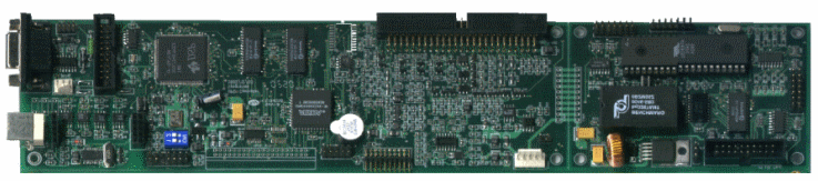
The TMS320F2407A running at 40 MHz with a single 3.3V supply voltage, this makes it a challenge in hardware design for electromagnetic interference reduction. Special design considerations must be carried out in the design of the PCBs for the power and control circuits for EMI control. Fig. 4.4 shows the picture of the designed DSP control card for 2U rack-mount UPS systems. This single-board DSP controller is designed to meet high-performance requirement for power electronic systems.

4.4 Development of the Power Board
Realization of the power board of an on-line UPS system includes a lot of accumulated experienced engineering works, such as on the components selection, design options for application models, power circuit PCB layout for EMI reduction, and safety requirements, etc.

4.5 System Integration
Fig. 4.5 shows the DSP-controlled UPS under development. The developed DSP control techniques have been realized into a commercialized 2kVA UPS to shows the feasibility of employing modern digital control techniques by using an advanced digital signal processor. A systematic top-down design procedure has been developed in the design of the a series of high-performance cost-effective UPS systems for rack-mount server applications.
4.6 Real-Time Control Firmware Design
The control of a power processing system is essential a real-time control problem. Many real-time control tasks can only be tested after the complete hardware has been constructed. It is time consuming for inexperienced engineers in developing these control, communication, and interface software for a commercialized UPS system. Fig. 4.7 shows the system software architecture of an on-line UPS. The control software are classified into three categories: real-time interrupted control routines, periodic background sequential control routines, and aperiodical background interface control routines. Fig. 4.8 illustrate the operating mode and interrupt mechanism of the DSP-based UPS controller and Fig. 4.9 shows the main flow chart of the system software. The interrupt-driven mechanism is activated by a real-time timer. An innovative asynchronous control scheme has been developed for the digital current loop control to achieve both good dynamic response and low electro-magnetic interference (EMI) with low PWM switching frequency.
6. Conclusions
This research has completed the design and implementation of a DSP-embedded fully digital-controlled single-phase on-line uninterruptible power supply (UPS) system. The applications of high-performance DSP in complicated power electronic systems will find great potential in synthesis of sophisticated control algorithms and PWM switching schemes. This paper has applied a single-chip DSP controller, the TMS320F2407A, in realizing all the required control functions for a single-phase on-line UPS. Experimental results show the designed 2 kVA UPS can reach very good dynamic responses both in utility interface and output voltage regulation.
Some practical important research issues include:
Fore more & Credits Goes goHere


